The 2nm GAA process offers a significant performance and efficiency boost over Samsung’s older manufacturing technologies. However, Samsung’s Foundry Vice President has emphasized that merely shrinking process nodes now yields only minor benefits. To overcome these limitations, the company believes it is essential to explore alternative approaches.
### Introducing Design and Process Integration Optimization (DTCO)
Samsung has proposed a method called **Design and Process Integration Optimization (DTCO)**. This approach focuses on researching and implementing modifications that can enhance the capabilities of cutting-edge nodes beyond what traditional scaling can achieve.
One critical area where Samsung has made notable improvements is the transition from **FinFET** to **Gate-All-Around (GAA)** structures. This shift maximizes current control capabilities and enables Samsung’s 2nm node to deliver significant enhancements in performance and efficiency.
### Industry Shift Toward DTCO
Speaking at the eighth Semiconductor Industry-Academia-Research Exchange Workshop held at COEX in Seoul, Samsung Electronics Foundry Vice President Shin Jong-shin explained that the semiconductor industry has increasingly shifted its focus towards DTCO. Both Samsung and its competitor TSMC have established dedicated teams to pursue simultaneous design and process innovations.
“Now, process miniaturization alone can only lead to improvements of 10-15%. As process performance improvement reaches its limits, the industry is paying attention to DTCO. At 7nm, approximately 10% of the overall performance improvement is due to DTCO. We expect that share to reach 50% at 3nm and below. Both Samsung and TSMC have dedicated DTCO teams and are pursuing simultaneous design and process improvements,” Shin stated.
### How DTCO Works
According to The Elec, DTCO involves engineers reviewing existing process constraints and exploring alternatives based on requests from designers, such as Tesla. By modifying fabrication processes, chip cells can be placed more efficiently, leading to reduced surface area and improved performance.
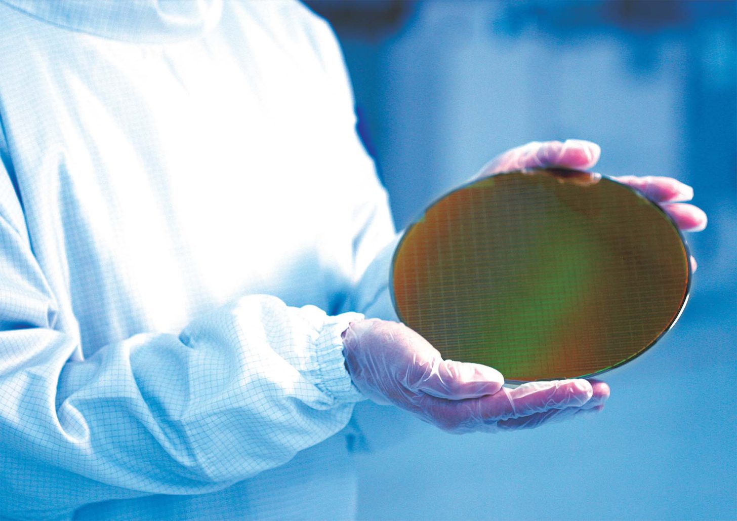
Samsung has already employed FinFET architecture on previous nodes and transitioned to GAA structures starting with its 3nm variant. Although the 3nm process faced challenges in yield, the newer 2nm node is showing great promise.
### Performance Gains at Smaller Nodes
Shin further highlighted that when moving from one node to the next, performance improvements and area reductions typically reach about 15%. While artificial intelligence fields may see performance doubling every few months, semiconductor process improvements are more incremental. “A 1-2% difference in performance is very important. Such differences can become decisive criteria for selecting a manufacturing process,” he added.
### Leveraging AI and Future Directions
In addition to exploring new design-process optimizations, Samsung is leveraging AI technologies to automatically generate new cell structures. These innovations aim to achieve smaller chip areas and reduce power consumption.
Looking ahead, Samsung plans to expand DTCO efforts into **System-Process Co-Optimization (SPCO)** and **System-Design-Process Co-Optimization (SDTCO)**. These expanded methodologies are expected to further refine semiconductor manufacturing and design.
### Current Status and Future Outlook
Samsung is reported to have completed the basic design of its second-generation 2nm GAA process. Its third iteration, known as SF2P+, is estimated to be implemented within the next two years. It is speculated that Samsung has extensively invested in DTCO to develop improved variations of its 2nm GAA process. This focus may explain the company’s decision to delay its 1.4nm node, opting instead to enhance its current process rather than directly competing with TSMC at that smaller node.
—
**News Source:** The Elec
https://wccftech.com/samsung-electronics-vp-says-process-miniaturaization-leads-to-negligible-improvements/